While silk screen seems like a small part of printed circuit board (PCB), it is actually an essential element in both the fabrication and assembly phases of the electronics. The white, or sometimes any other color, layer that is applied to the top of a PCB which contains valuable information needed for assembling and testing the circuit board. The80s:Why the silk screen is necessary for PCB production
Assembly - Identification And Instruction
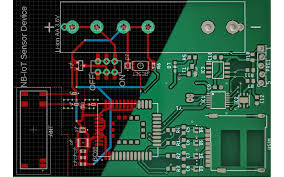
Component Labeling: Labels of the component like resistance, capacitor and IC are printed on the PCB with the help of silk screen. These names are not just any text. Otherwise, these texts have a certain nomenclature which in itself a coding system, to be specific, resistor values or capacitor ratings. For one thing, you might spot a part labeled as R1 1k, meaning this is the first 1 kilo-ohm resistor. Especially within manuel and automatic assembly processes this labeling is important to keep the correct placement of components.
Orientation Marks: Besides component labels, silk screen can include an orientation mark that indicates the direction in which polarized components such as diodes and capacitors should be placed. These markers are very important to help prevent assembly errors, such as placement errors that can result in fatal circuit failures, such as a reverse-mount error.
Improved Readability & User-friendliness
Test Points and Debugging information : to test and debugging, silk screen provide the Fabricators with some specific points in the PCB board, to ease maintenance. These pads provide a place to attach test equipment and to check operation as assembly proceeds and the final operation of the PCB as a whole.
User Interface Elements: In PCBs forming part of a user interface (like in consumer electronics) the silk screen can have symbols, icons or texts that provide instructions for users on how to interact with the device. As an example, this could be for a button to turn something on/off, especially a volume control or LED indicators which improve overall usability of the end product.
Quality and Aesthetics
Aesthetic Enhancement: If you are going to use silk screen on your PCB, then your PCB will automatically look clean and very professional. In consumer electronics (for which there may be a possibility for internal components to be seen by the eye operating through a transparent panel which may cause the LED lighted area inside the chassis emitting undesirable light patterns) this is especially necessary.
Durability and Protection
The Protection Layer: Protective Layer: Whileis secondary to its main application, the silk screen layer to some extent provides protection against mechanical friction and small chemical spill scenarios that could happen during the process of assembling.
Standards and Safety Information
Dream Green DIYUses Silk Screens For Printing Compliance MarksOn some products, The compliance mark, like undergoing standards for European conformity (CE mark), of for complying with safety standards (UL mark) is a huge and vital detail |YGONorthmontNature},"...priBehokeepTheuse of silk screens can also help print compliance markings on the product itself - such as CE mark for ensuring conformity to European standards, or UL mark for conforming to safety standards on electronics, on some of these products the compliance mark is a big deal and it means a lot. In certain markets and for certain applications, these markings are mandatory for PCBs, to guarantee that products comply with regulations.
Customization and Optimization
Manufacturers can make good use of this screen by selecting the suitable ink and print methods according to the PCB requirements. For example, UV-curable inks can provide much more lasting results, and and multiple colors can be used to separate different types of information more distinctly.
The silk screen is not just another layer of ink; it is an essential element that adds functionality, improves usability, and guarantees compliance in PCB manufacturing. For more information about the application and advantages of silk screen, visit silk screen This understanding will help you grasp the intricacies of the PCB design and manufacturing field, and show you why even the smallest detail in electronic technologies count for a lot.